Objectives:
To program and use the ADC feature of ATmega16
Show the lower byte of ADC digital value on Port D and higher byte on Port B
Introduction:
ADC is used to convert the analog voltages into digital value. ADC is widely used in data
acquisition so most of the modern microcontrollers have on-chip ADC peripheral. ATmega16
has on-chip ADC of 10-bit resolution. It has 8 analog input channels, out of which 7 input
channels can be used for differential input. Two differential input channels (ADC0 and ADC2)
can have the input gain of 10x and 200x.
As the ADC is 10-bit, so the converted digital output is stored in two 8-bit registers ADCL and
ADCH. Reference voltages for ADC can be connected to AVCC (Analog Vcc), internal 2.56V
reference or external AREF pin. Minimum 0V and maximum Vcc
can be converted to a digital
value. Successive approximation circuitry converted and analog voltage into digital value. This
circuitry requires a clock frequency between 50 kHz to 100 kHz.
Important Registers Associated with ADC:
Following five registers are associated with the ADC of AVR:
ADCL : Has 8 LSBs of converted digital result
ADCH : Has 2 MSBs of converted digital result
ADMUX : For left / right adjusted result, reference voltage and channel selection
ADCSRA : ADC control and status register
SFIOR : Three MSBs of this register are used to select the auto trigger source of ADC
Single ended result can be found from following formula:
ADC=Vin× 1024
Vref
where Vin is the voltage on the selected input channel, Vref the selected voltagereference and ADC is the 10-bit converted digital decimal value.
Similarly, differential input result can be found from following formula:
ADC=(Vpos −Vneg ) ×Gain × 512
Vref
where Vpos and Vneg are the two differential input channels and the Gain can be selected as 1x, 10x and 200x from ADMUX register.
Bit # 7 6 5 4 3 2 1 0
Bit Name REFS1 REFS0 ADLAR MUX4 MUX3 MUX2 MUX1 MUX0
REFS1:0 Reference selection bits
0 0 AREF, Internal Vref turned off
0 1 AVCC with external capacitor at AREF pin
1 0 Reserved
1 1 Internal 2.56V Voltage Reference with external capacitor at AREF pin
ADLAR :- ADC Left Adjusted Result. When this bit is set, ADCL contains only two LSBs of
the result at position D7 and D6. Remaining bits are not used
MUX4 : 0 :- Analog channel and gain selection bits. See following table for details
ADMUX (ADC Multiplexer Selection Register)
MUX4:0 Single EndedI/P Positive Differential I/P Negative Differential I/P Gain 00000 ADC0
00001 ADC1
00010 ADC2
00011 ADC3
00100 ADC4
00101 ADC5
00110 ADC6
00111 ADC7
01000* NA
ADC0 ADC0 10x
01001 ADC1 ADC0 10x
01010* ADC0 ADC0 200x
01011 ADC1 ADC0 200x
01100* ADC2 ADC2 10x
01101 ADC3 ADC2 10x
01110* ADC2 ADC2 200x
01111 ADC3 ADC2 200x
10000 ADC0 ADC1 1x
10001* ADC1 ADC1 1x
10010 ADC2 ADC1 1x
10011 ADC3 ADC1 1x
10100 ADC4 ADC1 1x
10101 ADC5 ADC1 1x
10110 ADC6 ADC1 1x
10111 ADC7 ADC1 1x
11000 ADC0 ADC2 1x
11001 ADC1 ADC2 1x
11010* ADC2 ADC2 1x
11011 ADC3 ADC2 1x
11100 ADC4 ADC2 1x
11101 ADC5 ADC1 1x
11110 1.22V(VBG) NA
11111 0V (GND)
* Not applicable
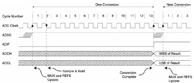
ADC Timing Diagram-Singal Conversion
Steps to program A/D converter using interrupts:
1. Make the pin input which is selected as ADC input channel
2. Turn ON the ADC module by setting ADEN of ADCSRA
3. Select the conversion speed using ADPS2:0 bits of ADCSRA
4. Load the appropriate value in ADMUX to select the input channel, reference voltages
and left of right aligned result.
5. Enable the ADC interrupt by setting ADIE bit of ADCSRA and D7 of SREG
6. Now start the conversion by setting ADSC bit of ADCSRA
7. Interrupt will be generated when conversion is done. First read ADCL then ADCH, if
result if right aligned
8. Go to step 6 to read the selected channel again
C Code to Display ADC value on Port A and Port B:
/* This program converts the analog input to 10-bit digital output. ADC0 (channel 0) is analog input. Lower byte of digital output is shown on Port D and 2 MSB bits out of 10 bits is shown on Port B */.
#include<avr\io.h>
#include<avr\interrupt.h>
/////////////// Macros Definition/////////////////
#define Bit(x) (0x01 << (x))
#define BitSet(p, m) ((p) |= (m))
#define BitClr(p, m) ((p) &= ~(m))
void InitADC(void);
ISR(ADC_vect)
{
PORTD = ADCL;
PORTB = ADCH;
BitSet(ADCSRA, Bit(6)); //Start conversion again
}
int main(void)
{
DDRA = 0x00; //PortA as input for ADC input
DDRD = 0xFF; //PortD as output for lower byte of Digital value
DDRB = 0xFF; //PortB as output for higher byte of Digital value
InitADC();
sei(); //Enable global interrupt
while(1);
}
void InitADC(void)
{
BitSet(ADMUX, Bit(7)); //Internal 2.56V selected as Vref
BitSet(ADMUX, Bit(6)); //Internal 2.56V selected as Vref
BitClr(ADMUX, Bit(5)); //Right adjusted result
BitClr(ADMUX, Bit(4)); //Single ended (GND as common ground)
BitClr(ADMUX, Bit(3)); //non-differential input on ADC0 channel (PA0, Pin No. 40)
BitClr(ADMUX, Bit(2)); //
BitClr(ADMUX, Bit(1)); //
BitClr(ADMUX, Bit(0)); //
//ADMUX = 0xC0; //Same settings as given above
BitSet(ADCSRA, Bit(7)); //Enable ADC
BitClr(ADCSRA, Bit(5)); //Disable Auto Trigger
BitSet(ADCSRA, Bit(3)); //Enable ADC Interrupt
BitSet(ADCSRA, Bit(2)); //Prescaler = Fosc/128
BitSet(ADCSRA, Bit(1)); //Prescaler = Fosc/128
BitSet(ADCSRA, Bit(0)); //Prescaler = Fosc/128
BitSet(ADCSRA, Bit(6)); //Start Conversion
//ADCSRA = 0xCF ; //Same settings as described above
}
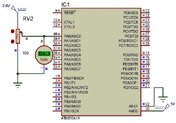
Simulation: