Introduction
Power diodes play a significant role in power electronics circuits for conversion of
electric power. A diode acts as a switch to perform various functions such as switches in rectifiers, freewheeling in switching regulators, charge reversal of capacitor and energy transfer between components, voltage isolation, energy feedback from the load to the power source and trapped energy recovery.
Constructional Considerations:
Power Diodes of greatest rating are required to conduct several kilo amps of current
in the frwd direction with very low loss while blocking several kilo volts in the
reverse direction. Large blocking voltage requires wide depletion layer in order to restrict the maximum electric field strength below the “impact ionization”. Charge
density(n) in the depletion region will be low in order to yield a wide depletion layer
for a given maximum fields strength. These requirements will be considered in
a lightly extrinsic doped p-n diode of wider width to accommodate the required
depletion layer. Such a construction will result in a device with high resistivity
in the forward direction. As a result, the power loss at rated current will
be unacceptably high.
On the other hand if forward resistance (and hence power loss) is reduced by increasing the doping level, reverse break down voltage will reduce. This apparent contradiction in power diode is solved by introducing a lightly doped “drift layer”
of required thickness between two heavily doped p and n layers.
Structure of Power Diode
The structure of the power diode is little different than the small signal diodes. Figure
shows the structure of power diode. In this figure observe that there is heavily doped
n substrate with doping level of 19 310 / cm. This substrate forms a cathode of the diode.
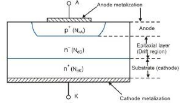
On n substrate, lightly doped n epitaxial layer is grown. This layer is also called drift region. The doping of n type junction layer is about 14 3 10 / cm.
Then the pn junction is formed by diffusing a heavily doped p region. This p-region forms the anode of the diode. The doping level of p-region is 19 310 / cm. The thickness of p region is 10 m . The thickness of n-substrate is 250 m . The thickness of ndrift layer depends upon the breakdown voltage of diode. For larger Vbd (breakdown), the drift region is wide. The n drift region is absent in low power signal diodes. The drift region absorbs depletion layer of the reversed biased pn.Conductivity modulation of the drift layer
Now let us see what will happen when the power diode is forward biased. Under this
condition, the holes will be injected from the p-region into the drift region. Some of the
holes combine with the electrons in the drift region. Since injected holes are large, they
attract electrons from the n-layer. Thus holes and electrons are injected in the drift
region simultaneously. Hence resistance of the drift region reduces significantly. Thus
diode current goes on increasing, but drift region resistance remains almost constant.
Hence on-state losses in the diode are reduced. This phenomena is called conductivity
modulation of drift region. This phenomena is present in almost all the power devices.
junction.