Objectives:
To program and use the PWM feature of ATmega16
To generate a square wave of 20% duty cycle using PWM feature of AVR
Introduction:
PWM has a wide variety of applications, ranging from measurement and communications to power control and conversion. One of the popular applications of PWM is the speed control of DC motors. By varying the duty cycle through PWM, speed of DC motor can be controlled for a fixed load. Higher the duty cycle, greater the speed of DC motor. AVR feature of PWM enables us to generate the square wave of desired frequency and pulse width (duty cycle). At the same time, we can perform the other task as the CPU is not busy in the wave generation.
PWM Modes:
ATmega16 has three timers which can be used as wave generation on their dedicated pins. There are two basic PWM modes, Fast PWM and Phase Correct PWM.
1- Fast PWM Mode:
In Fast PWM, the TCNT0 counts like it does in Normal Mode. After the timer is started, it starts to count up. Whenever it rolls over from its Top (0xFF in Timer0) to 0x00, TOV0 flag is raised. It can be selected by using COM01:00 bits of TCCR0 whether to set or clear the OC0 pin after the TOV0 flag is raised. While counting from Bottom to Top, compare match occurs when TCNT0
matches OCR0 and on the compare match, OC0 pin can be programmed to set or clear. For non-inverted Fast PWM mode, upon compare match, OC0 pin clears and upon Top (0xFF)
of TCNT0, OC0 pin sets. For inverted Fast PWM mode, upon compare match, OC0 pins sets and upon Top (0xFF) of TCNT0, OC0 pin clears. Both of these modes of Fast PWM can be
understood from the Fig .
Value to be loaded in OCR0 to generate the PWM of required duty cycle can be determined from the following formula:
Duty Cycle= OCR0 + 1 x 100 Non-Inverting mode
256
Duty Cycle=255-OCR0 x 100 Inverting mode
256
WGM01:00 bits of TCCR0 register are used to select the different modes of timer.
Bit # 7 6 5 4 3 2 1 0
Bit Name FOC0 WGM00 COM01 COM00 WGM01 CS02 CS01 CS00
Read/Write:W RW RW RW RW RW RW
Initial value 0 0 0 0 0 0 0
RW
0
FOC0 Force Output Compare: FOC0 bit is only active when the WGM00:1
bits specifies a non-PWM mode.
WGM00 WGM01 Timer Mode 0 Selector Bits (Four modes available)
0 0 Normal Mode
0 1 CTC (Clear Timer on Compare Match) Mode
1 0 PWM, Phase Correct Mode
1 1 Fast PWM
COM01 : COM00 Compare Output Mode: used to select the following operation if Fast
PWM is selected through WGM01:00:
0 0 Disconnect, Normal port operation, OC0 disconnected
0 1 Reserved
1 0 Non-inverted, Clear OC0 on compare match, set OC0 at Top
1 1 Inverted, Set OC0 on compare match, clearOC0 on Top
CS02:00 D2 D1 D0 Timer 0 Clock Source Selector
0 0 0 No clock source (Timer/Counter stopped)
0 0 1 clk (No Prescaling)
0 1 0 clk / 8
0 1 1 clk / 64
1 0 0 clk / 256
1 0 1 clk / 1024
1 1 0 External clock on T0 (PB0) pin. Clock on falling edge
1 1 1
External clock on T0 (PB0) pin. Clock on rising edge
TCCR0 (Timer / Counter Control Register)
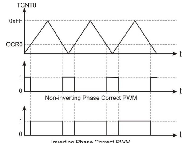
2- Phase Correct PWM Mode:
In Phase Correct PWM Mode, the TCNT0 goes up and down like a yo-yo. After the timer is started, it starts to count up and after reaching Top, it counts downward. Whenever it reaches to
0x00, TOV0 flag is raised. TCNT0 meets the OCR0 two times, one while counting upward and second while counting downward. It can be selected by using COM01:00 bits of TCCR0.
whether to set or clear the OC0 pin after compare match is occurred while counting upward.
Similarly, while counting downward, on the compare match, OC0 pin can be programmed to set
or clear. In non-inverted phase correct mode, OC0 pin is cleared when compare match occurs
while TCNT0 is counting upward and set OC0 pin when compare match occurs while TCNT0 is
counting downward. Reverse is the case from Inverted phase correct PWM. Both of these
modes of Phase Correct PWM can be understood from the Fig.
Value to be loaded in OCR0 to generate the PWM of required duty cycle can be determined
from the following formula:
Duty Cycle = OCR0 x 100 Non-Inverted Mode for Phase correct
255
Duty Cycle=255-OCR0 x 100 Inverted mode for phase correct
255
In TCCR0, Phase Correct PWM Mode can be selected by WGM01:00 = 01. For Phase Correct
PWM Mode, COM01:00 bits of TCCR0 performs the following operation:
COM01:00 Mode Operation
0 0 Normal Normal port operation, OC0 disconnected
0 1 Reserved
1 1 Non-inverting Clear OC0 on up-counting compare, Set OC0 on down-counting compare
1 1 Inverting Set OC0 on up-counting compare, Clear OC0 on down-counting compare
As Timer2 is also 8-bit timer, therefore it works similar to Timer0. The differences are the
register names, output pin and the prescaler of TCCRx register. For Timer0 and Timer2 the Top
is fixed (0xFF).
Timer1 is a 16-bit timer. Modes of Timer1 can be selected from TCCR1B TCCR1A registers.
Details of PWM generation through Timer1 are beyond the scope of this lab. However, the basic
principle is same as discussed earlier.
ICNC1 D7 Setting this bit enables the input noise canceller
ICES1 D6 Setting this bit enables the input capture on falling edge
WGM00 WGM01 Timer1 Modes (WGM11:10 are in TCCR1A)
Mode
WGM
Timer/Counter Mode of Operation Top Top Type
Update of
OCR1x
TOV Flag
Set on
13 12 11 10
1 0 0 0 0 Normal 0xFFFF Fixed Immediate Max
2 0 0 0 1 PWM, Phase Correct, 8 bit 0x00FF Fixed Top Bottom
3 0 0 1 0 PWM, Phase Correct, 9 bit 0x01FF Fixed Top Bottom
4 0 0 1 1 PWM, Phase Correct, 10 bit 0x03FF Fixed Top Bottom
5 0 1 0 0 CTC OCR1A Variable Immediate Max
6 0 1 0 1 Fast PWM, 8 bit 0x00FF Fixed Top Top
7 0 1 1 0 Fast PWM, 9 bit 0x01FF Fixed Top Top
8 0 1 1 1 Fast PWM, 10 bit 0x03FF Fixed Top Top Top
9 1 0 0 0 PWM, Phase & Frequency Correct ICR1 Variable Bottom Bottom
10 1 0 0 1 PWM, Phase & Frequency Correct OCR1A Variable Bottom Bottom
11 1 0 1 0 PWM, Phase Correct ICR1 Variable Top Bottom
12 1 0 1 1 PWM, Phase Correct OCR1A Variable Top Bottom
13 1 1 0 0 CTC ICR1 Variable Immediate Max
14 1 1 0 1 Reserved - - - -15 1 1 1 0 Fast PWM ICR1 Variable Top Top
16 1 1 1 1 Fast PWM OCR1A Variable Top Top
CS12:10 D2 D1 D0 Timer 1 Clock Source Selector
0 0 0 No clock source (Timer/Counter stopped)
0 0 1 clk (No Prescaling)
0 1 0 clk / 8
0 1 1 clk / 64
1 0 0 clk / 256
1 0 1 clk / 1024
1 1 0 External clock on T1 (PB1) pin. Clock on falling edge
1 1 1 External clock on T1 (PB1) pin. Clock on rising edge
TCCR1B (Timer1 Control Register B)
C Code for PWM generation using Fast PWM Mode:
/*
This program generates the square wave of 20% duty cycle on OC0 pin of ATmega16 using
the PWM feature of AVR. We would use Fast PWM mode of complete this task
For fast PWM non-inverted mode, formula is as follows:
Duty Cycle = (OCR0 + 1)/256*100
20*256/100 = OCR0 + 1
51 = OCR0 + 1
OCR0 = 50 = 0x32
So, we will load 0x32 in ORC0 in order to generate square wave, having 20% duty cycle
*/
#include<AVR\io.h>
void main(void)
{
DDRB = 0xFF; //Make PortB as output to generate PWM on OC0 (PB3)
OCR0 = 0x32; //to generate 20% duty cycle
TCCR0 = 0x69; //Configure fast PWM, non-inverted, without prescaler
while(1);
}
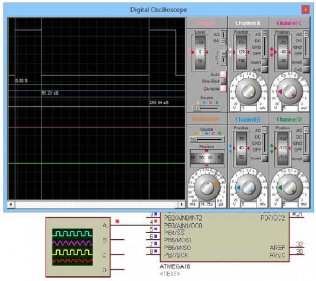
Simulation: