Experiment
Aim of the experiment
i. To understand the basic circuit and operation of a simple Boost Converter.
ii. To study Continuous, Discontinuous and Boundary Conduction Modes of the Boost
Converter by varying.
a. Duty cycle
b. Switching frequency
c. Load
Required components and equipments
1. MOSFET Irf740
2. Driver IC IR2110
3. Inductor
4. Capacitor
5. Diode
6. Resistive load
Theory
A DC-DC converter(chopper) is a device that accepts a DC input voltage and produces a DC output
voltage. Typically the output produced is at a different voltage level than the input. In addition,
DC-to-DC converters are used to provide noise isolation, power bus regulation, etc. Here we are
going to study boost converter.
A boost converter (step-up converter) is a power converter with an output dc voltage greater
than its input dc voltage. Since power (V*I) must be conserved, the output current is lowered
from the source current. It is a class of switching-mode power supply (SMPS) containing at
least two semiconductor switches (a diode and a transistor) and at least one energy storage
element. Filters made of inductor and capacitor combinations are often added to a converter’s
output to improve performance. Fig 2.1 shows the power circuit schematic of a boost converter.
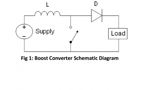
Boost Converter Schematic Diagram
The basic principle of a boost converter consists in 2 distinct states .
1) In the On-state, the switch SW is closed, resulting in an increase in the inductor
current.
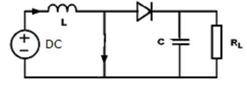
Fig.2 Switch is closed
2) In the Off-state, the switch is open and the only path offered to inductor current is through the
fly back diode D, the capacitor C and the load R. It results in transferring the energy
compilrd on the On-state into capacitor.
Fig.3 Switch is open
The boosting of voltages in the boost converter can be related through the following
equation
Vo = Vi
/ (1-D)
The above relation shows that in case of D=0 there will be no boosting.
Note: Avoid D=0 and D=1 keep the range of duty cycle 10 % to 90 %
Procedure
Construct the circuit as shown in the fig.1. Do the changes as instructed below.
Varying Duty Cycle
Set the duty ratio at 50%, switching frequency at 100kHz and RL
= 1kΩ.
1. Vary the duty ratio from 10 % to 90 % (in steps of 10%). Draw the input and output wave
forms.
2. Measure the average output voltage for the corresponding duty ratio.
3. Calculate the theoretical average output voltage for the corresponding duty ratios.
Varying the frequency
1. Set the duty ratio to 50 %.
2. Measure the peak-peak output ripple voltage.
3. Repeat the above procedure for different switching frequencies (1kHz, 2kHz, 3kHz). Draw the
corresponding input and output wave forms.
Circuit1
Fig. 4 Boost converter
Observation:
Varying Duty Cycle
Observe and make a copy of the switch input voltage, output ripple voltage, output current and
capacitor current waveforms.
Varying Duty Cycle
Observe and make a copy of the sw input voltage, output ripple voltage, output current and
capacitor current waveforms and draw it on the given graph paper.
S.No Vin Vo f δ L C Load Ripples Remarks
1.(H)
1.(S)
2. (H)
2.(S)
3. (H)
3.(S)
Varying the frequency
Observe and make a copy of the switch input voltage, output ripple voltage, the output current
and capacitor current waveforms and draw it on the given graph.
Varying Duty Cycle
Observe and make a copy of the sw input voltage, output ripple voltage, output current and
capacitor current waveforms and draw it on the given graph paper.
S.No Vin Vo f δ L C Load Ripples Remarks
1.(H)
1.(S)
2. (H)
2.(S)
3. (H)
3.(S)
Conclusion :