The BJT's constructed with three doped semiconductor regions separated by two pn junctions, as shown in the epitaxial planar structure in Figure –1(a). The three regions are called emitter, base, and collector. The two types of BJTs are shown in Figure –1(b) and (c). One type consists of two n regions separated by a p-region (npn), and the other type consists of two p regions separated by an n-region (pnp). The term bi-polar refers to the use of both holes and electrons as current carriers in the transistor structure.
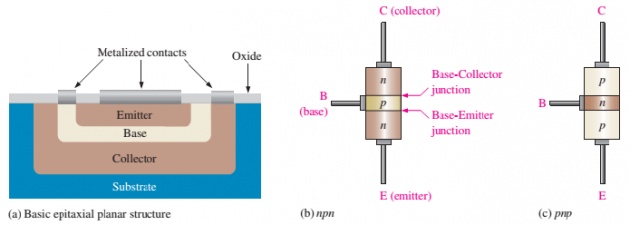
The p-n junction joining the base region and the emitter region is called the base-emitter
junction. The p-n junction joining the base region and the collector region is called the
base-collector junction, as indicated in Figure –1(b). A wire lead connects to each of the three regions, as shown. These leads are labeled E(emitter), B(base), and C(collector). The B(base) region is lightly doped and very thin compared to the heavily doped emitter and the moderately doped collector regions. Figure –2 shows the schematic symbols for the npn and pnp bipolar junction transistors.
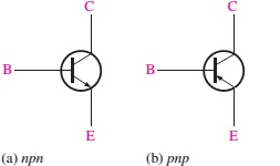
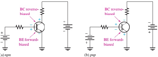
Figure –3 shows a bias arrangement for both npn and pnp BJTs for operation as an amplifier .Notice that in both cases the base-emitter (BE) junction is forward-biased and the base-collector (BC) junction is reverse-biased. This condition is called forward-reverse bias.
For operation of transistor, let’s examine what happens inside the npn structure. The n-type(heavily doped) emitter region has a very high density of conduction-band (free) electrons, as indicated in Figure –4. These free e's easily diffuse through the frwd bias BE junction into the lightly doped and very thin base region, the wide arrow. The base has a small number of holes. A low %age of total number of free electrons entered into the base region combine with holes and move as valence electrons through the base region and into the emitter region as hole current.
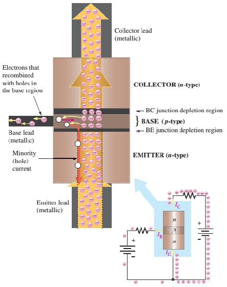
When the electrons that have recombined with holes as valence electrons leave the crystalline structure of base(B), they become free in the metallic base and produce the base current(Ib). Most of the electrons that have entered the base(B) do not recombine with holes because the base is very thin. As for as, the electrons move toward the BC junction, they are swept across into the collector region by the attraction of the +ive collector VCC. The free electrons pass toward the collector region, into the external circuit, and then return into the emitter region along with the base current, as indicated. The emitter current is slightly greater than the collector current because of the small base current that splits off from the total current injected into the base region from the emitter.