PCB stands for "Printed Circuit Board"
What is PCB?
PCB basically base on electrically and mechanical components using Tracks,Pads and other features which are mount by removing cooper from the cooper sheet.
It is very rugges,highly reliable and inexpensive.It may be one layer,two layer and multilayers.When PCB sheet is mounted with components it is call populated and without components it is called bare PCB.
Why we need a PCB?
PCB is used for making circuits. Those circuits which we are used in Hardware.It is lower cost quantity production.
It take less time to design a circuit.Mounting of components and wiring can be done easily. Now a days this is done through meachines which is very fast and well looked.
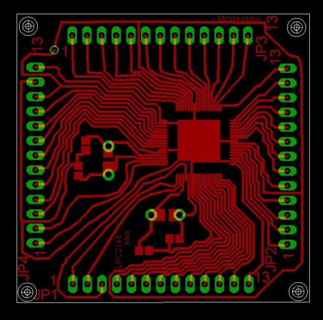
What is the Parts of PCB?
These are main components of a PCB.
1-Components
2-Pads
3-Tracks
4-Vias
5-Top Layer
6-Bottom Layer
7-Jumpers
8-Silk Screen
Components:
There is mainly two types of components are availabe for PCB
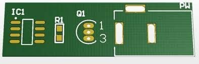
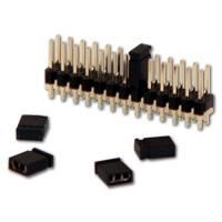
1-Through Hole Technology (THT)
These componenets are insterted in the holes and solder from one or both sides of PCB.This types of components required much space on PCB.
Following picture shows the THT components
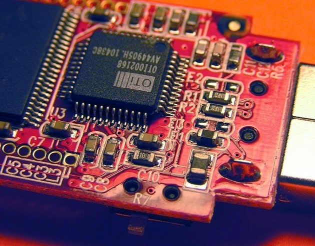
2-Surface Mount Technology (SMT)
These componenets are placed on PCB and can be mount on both sides of PCB.This types of components required very small space on PCB.
These components are cheaper and used for multilayers PCB.
Following picture shows the SMT components
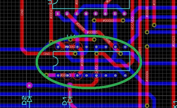
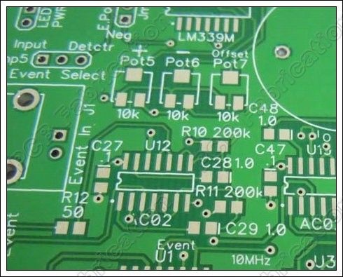
PADs:
Pads are the location where the the components are connected.These pads are connected with tacks. THT pads are drilled but SMT pads don't have to drills.
Following picture shows the PADs of PCB
Tracks:
Tracks are the copper path through which current flows and give the power to components which are mount on pads.
As the high current needed wide enough tracks and low current required less width.
Following picture shows the Tracks
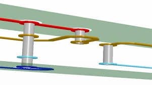
Vias:
It is used for connecting different layers with each other in PCB. Try to minimum use of Vias.
Following picture shows the Vias
Top Layer:
When we design a PCB which is only one sided then this side is called Top layer and this side will be solder.
On top layer very few components are placed.Most of the tracks are routed on this layer
Most of the soldering is done on this layer.
Bottom Layer:
There are very few traces on the bottom layer and many of the components are reside on this layer.
Single side PCB has no bottom layer.
Following picture shows the Top & Bottom Layer
Jumpers:
When we are going to design a very large and complex circuit then there will be some wire which are cross with each other. So therefore we used jumpers.
There are two types of Jumpers
1-Removable Jumpers
These types of jumpers easily remove from the PCB which named as Configuration Jumpers.
Following picture shows the Removable Jumpers
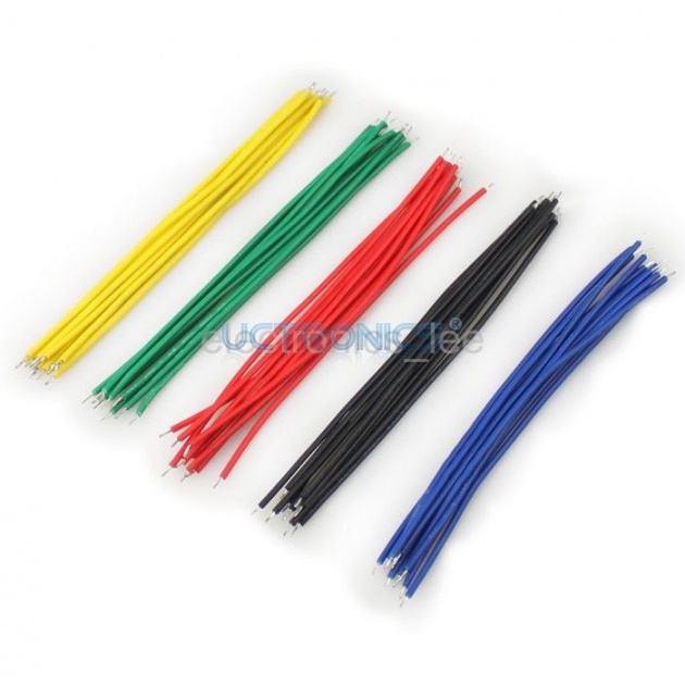
2-Fix Jumpers
Mostly this type of jumper are used in PCB. wires are used for this purpose.
Following picture shows the Fix Jumpers
Silk Screen:
Printed on the components side of PCB to designate the location of components.It is used to read information about components part and placement on PCB.It is helpful in assembly of components.
Following picture shows the Silk Screen
So these are the parts of PCB.
Source:
Workshop on PCB
Deliver By:
Engineer Muhammad Muzammil
Written By:
Ihtasham Zahid