Unipolar transistor
 911electronic.com/wp-content/uploads/2015/12/IMG_20151218_103902-768x576.jpg 768w, 911electronic.com/wp-content/uploads/2015/12/IMG_20151218_103902-1024x768.jpg 1024w" alt="unipolar transistor" width="340" height="255" />
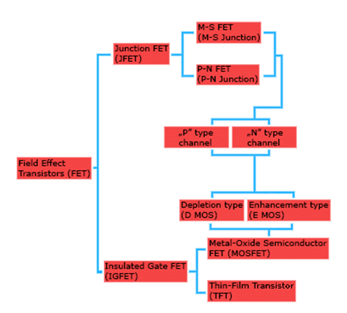
Unipolar Transistor (also known as Field-Effect Transistor – FET) –tri-ended (tri-electrode), semiconductor electronic component that has the ability to enhance the electrical signal. They transfer only one type of carriers: majority carriers (hence the name – unipolar), while the control of output current is done with use of electric field (field effect transistors). Depending on the operating laws, we can distinguish two main types of field effect transistors: Junction FET (JFET) and Insulated Gate FET (IGFET). The latter are divided into metal-oxide semiconductor FET (MOSFET) and Thin-Film Transistors (TFT).
The division of field effect transistors:
 911electronic.com/wp-content/uploads/2015/12/Screenshot_1.png 494w" alt="division of field effect transistors" width="294" height="265" />
Construction and rules of operation of field-effect transistors:
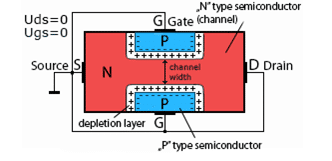
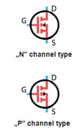
Unipolar Transistors have three electrodes: D – drain, G – gate, and S – source; these are equivalents to the electrodes occurred in bipolar transistors. Two of them:Drain and Source are connected to the properly doped crystal semiconductor. Between these ends channel is created through which the current flows. Third end is placed along the channel: Gate, thanks to which we control the flow of the current. In case of connecting multiple MOS transistors in an integrated circuit, fourth electrode is often used: B – Body (or Bulk) in order to bias the substrate. But in general this end is connected with the source.
Unipolar transistors operating states:
There are three operating modes of the transistors:
Cutoff mode: |UGS| > |UT| at any |UDS|,
Active mode (also known as the linear or unsaturated): |UGS| < |UT| and |UDS| <= |UDSsat|,
Saturation mode: |UGS| < |UT| and |UDS| => |UDSsat|.
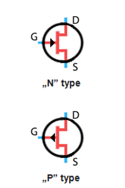
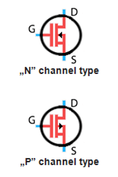
FET symbols:
JFET (normally on):
 911electronic.com/wp-content/uploads/2015/12/Screenshot_3.png 332w" alt="Jfet inner structure" width="332" height="161" />
In JFET transistors the gate is insulated from the channel by the reverse bias junction (very high input resistance). We meet two variants of this junction:
P-N junction (PNFET)
M-S junction (Metal-Semiconductor)
The channel through which the current will flow is located between the drain and source. One can control the width of the channel (its resistance) by changing the gate-source voltage (UGS). The increasing UGS voltage, which reverse bias the junction causes narrowing of the channel until the complete closure – the current won’t flow. To the UGSvoltage, the voltage drop between a specific point of channel and the source (UDS) is added. Increasing the UDS voltage value will ultimately connect depletion layers and closure the channel by saturating the transistor. The value of Drain current ID ceases to grow regardless of further increasing the UDS voltage, and transistor becomes a very good transconductance component.
MOSFET:
Depletion type – D MOS (normally on):
Enhancement type – E MOS (normally off):
 911electronic.com/wp-content/uploads/2015/12/Screenshot_6.png 321w" alt="Mosfet structure" width="321" height="166" />
In this type of transistors the gate is insulated from the channel with dielectric layer. The area marked “N+” is heavily doped “N” type semiconductor. In case of E MOS transistors with voltage of UGS = 0, channel is blocked (its resistance takes the value of MΩand the ID current doesn’t flow). By increasing the UGS voltage channel increases its conductivity and after reaching a certain value called UT threshold voltage, the flow of the ID drain current was possible through the channel.
The minimum resistance value of the channel specified by the manufacturer can be found in datasheets as rdson(it’s dependent from the maximum voltage of the UDS transistor. The value of ID current that will flow through the created channel is dependent from the UDS voltage, but it isn’t a linear relation. It’s described by the formula:
β– current amplifier ratio
This current affects on the gate bias state by changing it, which results in a narrowing of the channel near the drain. In case of further increasing the gate-source UGS voltage, the cut-off of UGSoff voltage will be exceeded at some point causing the loss of created channel (UGS= UDS)
The basic parameters of unipolar transistors:
UDSmax – the maximum drain-source voltage,
IDmax– the maximum drain current,
UGSmax– the maximum gate-source current,
Ptotmax– permissible power loss,
UP– the threshold voltage at which current begins to flow,
IDSS(UGS=0) – the saturation current at determined UDS current,
gm [S-Siemens] – transconductance ratio,
rds(on)– the minimum resistance value of the channel of transistor operating in the unsaturation mode,
IGmax– the maximum allowable gate current,
ID(OFF)– the drain current in cut-off mode – at a voltage | UGS| > | UGS(OFF)|.
Current-voltage characteristics of unipolar transistors:
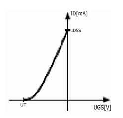
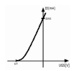
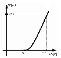
Transfer characteristics – it describes the relation of ID drain current from the gate-source UGS voltage with determined drain-source UDS voltage.
JFET “N”:
D MOS “N”:
E MOS “N”:
Drain characteristics (for “N” type unipolar transistors) – it describes the relation of drain IDcurrent from the drain-source UDSvoltage with determined gate-source UGSvoltage. The characteristics area was divided into two parts: the active and saturated scope.
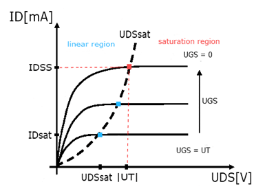 911electronic.com/wp-content/uploads/2015/12/Screenshot_10.png 385w" alt="Unipolar characteristics" width="385" height="278" />
Source: 911electronic.com/unipolar-transistor/